Triangular Honeycombs: Physicists design novel quantum material
Topological quantum materials with distinctive advantages
Researchers from the Würzburg-Dresden Cluster of Excellence ct.qmat–Complexity and Topology in Quantum Matter – have conceived and realized a new quantum material: "Indenene". Consisting of a single layer of the chemical element indium, indenene enriches the family of the so-called topological insulators. The triangular lattice behind its tailor-made materials-design concept is not only novel in the context of topological quantum materials but it also offers important advantages for future applications. Ever since the discovery of the first topological insulator this class of materials has been attributed enormous potential for the development of future electronics.
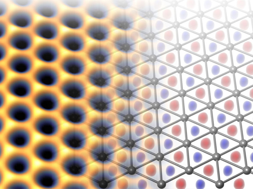
The measured electronic density (left) on the triangular indium lattice (right). The figure highlights how electrons (in yellow) do not sit on the atomic position but they rather occupy the voids in between (red and blue).
ct.qmat
Smartphones, notebooks and other electronic devices of our everyday life strongly benefit from the ever-increasing miniaturization of semiconductor devices. This development comes however at a price: confining electrons enhances their scattering– cell phones heat up.
Topological insulators hold promises for a more efficient and sustainable technology. At odds with conventional semiconductors, the current flows on their boundaries, with scattering becoming prohibited thanks to symmetry reasons. In other words, things stay cool! In 2007 Laurens Molenkamp, physicist at the University of Würzburg and member of the Cluster of Excellence, discovered the first topological quantum material, generating a worldwide resonance in the scientific community.
Indenene–a hidden honeycomb
In the search for new topological materials, most of the theory efforts hitherto have been focusing on two-dimensional atom layers in a honeycomb arrangement. The motivation comes from graphene, the "Drosophila" of the quantum spin Hall systems, or more simply, a single layer of the famous graphite inside our old-style classical pencils. The research team in Würzburg pursued instead an alternative route: the theoretical physicists around Giorgio Sangiovanni have proposed to use a simpler triangular atomic lattice.
This idea has been put into practice by the experimental team of Ralph Claessen, spokesperson of ct.qmat's Würzburg branch. Using state-of-the-art molecular beam techniques, the researchers succeeded in depositing a single layer of indium atoms as triangular lattice on a silicon carbide crystal as support – resulting in indenene. Thanks to this new combinations of building blocks and chemical elements, the relevant electrons do not localize directly on the indium positions but prefer to occupy thefree space in between them. From the perspective of the electrons their charge fills the "negative" of the triangular indium lattice which is actually a honeycomb lattice – hidden in the voids of the atomic structure.
Project head Giorgio Sangiovanni explains this through the quantum mechanical nature of particles: "One can describe the indium electrons as waves that pile up in the voids of the triangular lattice where at first sight you would not expect them to be. Interestingly, the resulting ‘hidden’ honeycomb connectivity leads to a particularly robust topological insulator, more than graphene."
Topological quantum materials with distinctive advantages
The unique materials design that has led to the synthesis of indenene can improve the current technological status in the field of topological electronics: In contrast to graphene, indenene needs not to be cooled down to ultra-low temperatures to manifest its properties as a topological insulator. This is a consequence of the particularly simple triangular lattice which allows for large structural domains, often a severe bottleneck in the synthesis of other topological materials.
"We were indeed surprised, that such a simple atomic structure can display topological properties. This is an essential asset for the successful growth of perfect indenene films that can meet the demanding standards required for device nanofabrication. Furthermore, the use of silicon carbide as supporting substrate allows us to connect to established semiconductor technology," says Ralph Claessen, commenting the scientific result.
Outlook
The simple structure of indenene represents at the same time a challenge: as soon as the single layer of indium atoms comes in contact with air, the material loses its special properties. For this reason the researchers are currently developing an atomic capping layer that can protect indenene from unwanted contamination during its synthesis. A solution to these issues will pave the way towards a large-scale use of these topological quantum materials.
