Crystal structures in super slow motion
Researchers first to succeed in filming a phase transition with extremely high spatial and temporal resolution
Laser beams can be used to change the properties of materials in an extremely precise way. This principle is already widely used in technologies such as rewritable DVDs. However, the underlying processes generally take place at such unimaginably fast speeds and at such a small scale that they have so far eluded direct observation. Researchers at the University of Göttingen and the Max Planck Institute (MPI) for Biophysical Chemistry in Göttingen have now managed to film, for the first time, the laser transformation of a crystal structure with nanometre resolution and in slow motion in an electron microscope.

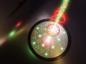
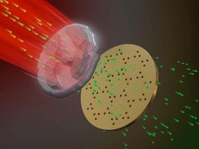
At the heart of the imaging technique is a complex array of 72 circular apertures
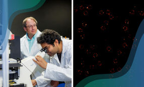
Dr Murat Sivis

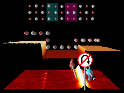
Artist's impression of the charge density wave in the ultrafast transmission electron microscope.
Dr Florian Sterl (Sterltech Optics)
The team, which includes Thomas Danz and Professor Claus Ropers, took advantage of an unusual property of a material made up of atomically thin layers of sulphur and tantalum atoms. At room temperature, its crystal structure is distorted into tiny wavelike structures - a "charge-density wave" is formed. At higher temperatures, a phase transition occurs in which the original microscopic waves suddenly disappear. The electrical conductivity also changes drastically, an interesting effect for nano-electronics.
In their experiments, the researchers induced this phase transition with short laser pulses and recorded a film of the charge-density wave reaction. "What we observe is the rapid formation and growth of tiny regions where the material was switched to the next phase," explains first author Thomas Danz from Göttingen University. "The Ultrafast Transmission Electron Microscope developed in Göttingen offers the highest time resolution for such imaging in the world today." The special feature of the experiment lies in a newly developed imaging technique, which is particularly sensitive to the specific changes observed in this phase transition. The Göttingen physicists use it to take images that are composed exclusively of electrons that have been scattered by the crystal's waviness.
Their cutting-edge approach allows the researchers to gain fundamental insights into light-induced structural changes. "We are already in a position to transfer our imaging technique to other crystal structures," says Professor Claus Ropers, leader of Nano-Optics and Ultrafast Dynamics at Göttingen University and Director at the MPI for Biophysical Chemistry. "In this way, we not only answer fundamental questions in solid-state physics, but also open up new perspectives for optically switchable materials in future, intelligent nano-electronics."
Original publication
Other news from the department science