Ionic defect landscape in perovskite solar cells revealed
The group of so-called metal halide perovskites as materials has revolutionized the field of photovoltaics in recent years. Generally speaking, metal halide perovskites are crystalline materials that follow the structure ABX3, with varying composition. Here, A, B, and X can represent a combination of different organic and inorganic ions. These materials have a number of properties that are ideal for use in solar cells and could help to make optoelectronic devices such as lasers, light-emitting diodes (LEDs), or photodetectors much more efficient. With regard to the development of a resource- and energy-efficient technology, the relevance of research on these materials is very high.
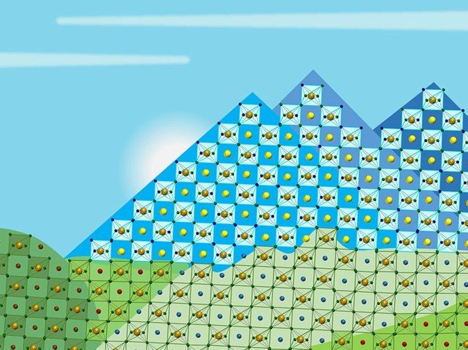
Artistic representation of an ionic defect landscape in the perovskites.
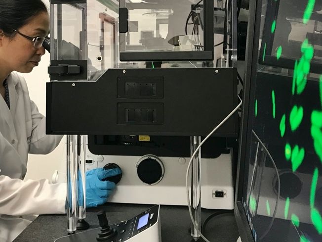
Prof. Dr. Yana Vaynzof (TU Dresden/cfaed)
The advantageous properties of metal halide perovskites include their high light-harvesting capacity and their remarkable ability to efficiently convert solar energy into electrical energy. Another special feature of these materials is that both charge carriers and ions are mobile within them. While charge carrier transport is a fundamental process required for the photovoltaic operation of the solar cell, ionic defects and ion transport often have undesirable consequences on the performance of these devices. Despite significant progress in this field of research, many questions regarding the physics of ions in perovskite materials remain open.
On the way to a better understanding of these structures, the Technical Universities of Chemnitz and Dresden have now taken a big step forward. In a joint investigation by the research groups around Prof. Dr. Yana Vaynzof (Chair of Emerging Electronic Technologies at the Institute of Applied Physics and Center for Advancing Electronics Dresden - cfaed, TU Dresden) and Prof. Dr. Carsten Deibel (Optics and Photonics of Condensed Matter, Chemnitz University of Technology) under the leadership of Chemnitz University of Technology, the two teams uncovered the ionic defect landscape in metal halide perovskites. They were able to identify essential properties of the ions that make up these materials. The migration of the ions leads to the presence of defects in the material, which have a negative effect on the efficiency and stability of perovskite solar cells. The working groups found that the motion of all observed ions, despite their different properties (such as positive or negative charge), follows a common transport mechanism and also allows the assignment of defects and ions. This is known as the Meyer-Neldel rule.
"Probing the ionic defect landscape of perovskite materials is not a simple task," says Sebastian Reichert, research assistant at the Chair of Optics and Photonics of Condensed Matter at Chemnitz University of Technology and lead author of the publication. "We needed to perform extensive spectroscopic characterization on perovskite samples in which the defects were intentionally introduced and their type and density were gradually tuned. Therefore, the expertise of both teams was invaluable," Reichert explains. Clarifying basic transport mechanisms
"One of the most important results of our study is the intricate interplay between the ionic and electronic landscapes in perovskite materials," adds Prof. Vaynzof, "By changing the density of the various ionic defects in perovskite materials, we observe that the built-in potential and the open-circuit voltage of the devices are affected." This highlights that defect engineering is a powerful tool to enhance the performance of perovskite solar cells beyond the state of the art.
The joint study also found that all ionic defects meet the so-called Meyer-Neldel rule. "This is very exciting since it reveals fundamental information about the hopping processes of ions in perovskites," says Prof. Deibel. "We currently have two hypotheses regarding the origin of this observation and we plan to investigate those in our future studies."
Original publication

Other news from the department science


Most read news


More news from our other portals


Last viewed contents
Robert_Gomer
Nanosafety research without animal experiments - Risk analyses for nanoparticles

Don't Give the Slightest Chance to Toxic Elements in Medicinal Products - New high-accuracy reference solutions for the SI-traceable measurement
Merck Secures All Antitrust Approvals for Sigma-Aldrich Acquisition - Completion of transaction expected in third quarter 2015

House cats’ noses may function like highly efficient chemical analysis equipment - Parallels between cat noses and gas chromatography provide new insights into mammalian evolution
New study about the global market for polyethylene-LLDPE - Flexible and robust
Dip-Pen_Nanolithography