Painting with crystals
Advertisement
semiconductors made of organic materials, e.g. for light-emitting diodes (OLEDs) and solar cells, could replace or supplement silicon-based electronics in the future. The efficiency of such devices depends crucially on the quality of thin layers of such organic semiconductors. These layers are created by coating or printing “inks” that contain the material. Researchers at the Max Planck Institute for Polymer Research (MPI-P) have developed a computer model that predicts the quality of such layers as a function of processing conditions, such as the drying time of the ink or the speed coating. This model aims to accelerate the time-consuming approaches for process and product optimization.
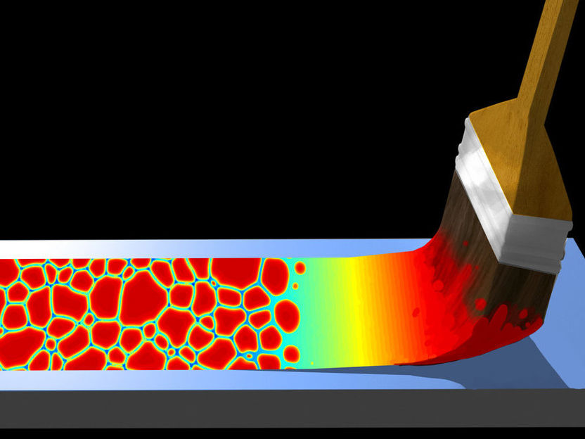
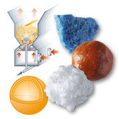
Using computer simulations, MPI-P scientists can predict the structure of crystals in organic semiconductor layers
© MPI-P
Organic semiconductors are used today for various electronic components, such as light-emitting diodes, solar cells and transistors. Where some of these applications are already widely used (OLEDs in particular), others still require substantial improvement before they can be introduced onto the market. Such components rely on the transport of electrons through the organic semiconductor. In the case of OLEDs, for example, electrons are supplied with energy by an electrical voltage, which they can then emit again in the form of light. However, if the quality of the organic layer is poor, much of the energy is returned to the material without emitting light.
An attractive way of manufacturing the semiconducting layers, is via printing or coating an ink containing the organic semiconductor in a solvent. During evaporation of the solvent the semiconductor forms crystals. The size and shape of these crystals determine the appearance and quality of the functional layer. “The optimal crystal size and shape are strongly application-dependent,” says Dr. Jasper J. Michels, lead author of the study and group leader in Prof. Paul Blom's department at the MPI-P. A big problem is that thus far it has not been possible to predict how the crystallization depends on the properties of the ink and the coating process. Hence, finding the fabrication strategy giving the best possible product performance is typically time-consuming, wasteful and expensive. “Not being able to predict the suitability of the coated layers prevents translating laboratory scale manufacture to industrial production and hampers wide spread new applications for organic electronics,” Michels explains.
A team of scientists led by Michels has now developed a computer model capable of making such predictions. The calculations mimic the actual coating and crystallization, as it happens real-time. By increasing the coating speed in their computer simulations, the authors demonstrated how the shape of the crystals exhibits a transition from ribbons, via elongated ellipsoids to small polygons. The simulations revealed that whether these shape transitions are sudden or gradual strongly depends on how quickly the solvent evaporates. “If we now know what role crystal-crystal interfaces play during the operation, our new model can pre-calculate the material- and process-settings to reach an optimal compromise between, for instance, production speed and film quality,” Michels explains. “We therefore hope that our work is an important step towards eventually making new products available based on organic semiconductors.”


