Broad spectrum: Novel hybrid material proves an efficient photodetector
Digital cameras as well as many other electronic devices need light-sensitive sensors. In order to cater for the increasing demand for optoelectronic components of this kind, industry is searching for new semiconductor materials. They are not only supposed to cover a broad range of wavelengths but should also be inexpensive. A hybrid material, developed in Dresden, fulfils both these requirements. Himani Arora, a physics PhD student at Helmholtz-Zentrum Dresden-Rossendorf (HZDR), demonstrated that this metal-organic framework can be used as a broadband photodetector. As it does not contain any cost-intensive raw materials, it can be produced inexpensively in bulk.

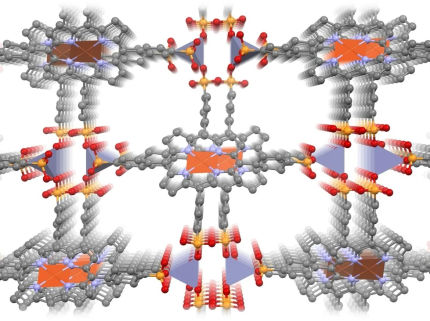
Physicists of HZDR and TU Dresden have developed a photodetector, which is completely based on layers of metal-organic frameworks. Since this compound can detect and transform a broad range of light wavelengths into electrical signals, it could become a novel detector material.
HZDR / Juniks
In the last twenty years, metal-organic frameworks (MOFs) have become a coveted material system. So far, these highly porous substances, up to 90 percent of which are composed of empty space, have largely been used to store gases, for catalysis or to slowly release drugs in the human body. “The metal-organic framework compound developed at TU Dresden comprises an organic material integrated with iron ions,” explains Dr. Artur Erbe, head of the "Transport in Nanostructures" group at HZDR’s Institute of Ion Beam Physics and Materials Research. “The special thing about it is that the framework forms superimposed layers with semiconducting properties, which makes it potentially interesting for optoelectronic applications.”
The group had the idea of using the new semiconducting two-dimensional MOF as a photodetector. In order to pursue it further, Himani Arora investigated the semiconductor’s electronic properties. She explored, among others, to what extent the light sensitivity was dependent on temperature and wavelength – and came to a promising conclusion: From 400 to 1575 nanometers, the semiconductor could detect a broad range of light wavelengths. The spectrum of radiation thus goes from ultraviolet to near infrared. “This is the first time we have proved such a broadband photodetection for a photodetector completely based on MOF layers,” the doctoral candidate notes. “These are ideal properties for using the material as an active element in optoelectronic components.”
Small bandgap makes for efficiency
The spectrum of wavelengths a semiconducting material can cover and transform into electrical signals essentially depends on the so-called bandgap. Experts use this term to describe the energetic distance between the valence band and the conduction band of a solid state material. In typical semiconductors, the valence band is completely full, so the electrons cannot move around. The conduction band, on the other hand, is largely empty, so the electrons can move around freely and influence the current flow. While the bandgap in insulators is so big that the electrons cannot jump from the valance band to the conduction band, metal conductors have no such gaps. A semiconductor’s bandgap is just big enough to raise the electrons to the higher energy level of the conduction band by using the light waves. The smaller the bandgap, the lesser the energy required to excite an electron. “As the bandgap in the material we explored is very small, only very little light energy is required to induce the electricity,” Himani Arora explains. “This is the reason for the large range of the detectable spectrum.”
By cooling the detector down to lower temperatures, the performance can be improved yet further because the thermal excitation of the electrons is supressed. Other improvements include optimizing the component configuration, producing more reliable contacts and developing the material further. The results suggest that the MOF-based photodetectors will have a bright future. Thanks to their electronic properties and inexpensive manufacturing, MOF layers are promising candidates for a raft of optoelectronic applications.
“The next step is to scale the layer thickness,” says Artur Erbe, looking forward. “In the study, 1.7 micrometer MOF films were used to build the photodetector. To integrate them into components, they need to be significantly thinner.” If possible, the aim is to reduce the superimposed layers to 70 nanometers, that is, 25 times smaller than their size. Down to this layer thickness the material should exhibit comparable properties. If the group can prove that the functionality remains the same in these significantly thinner layers, they can then embark on developing it to the production stage.
Original publication
Other news from the department science

Get the chemical industry in your inbox
By submitting this form you agree that LUMITOS AG will send you the newsletter(s) selected above by email. Your data will not be passed on to third parties. Your data will be stored and processed in accordance with our data protection regulations. LUMITOS may contact you by email for the purpose of advertising or market and opinion surveys. You can revoke your consent at any time without giving reasons to LUMITOS AG, Ernst-Augustin-Str. 2, 12489 Berlin, Germany or by e-mail at revoke@lumitos.com with effect for the future. In addition, each email contains a link to unsubscribe from the corresponding newsletter.
Most read news
More news from our other portals
Last viewed contents
Adam_of_Bodenstein

First realization of an electric circuit with a magnetic insulator using spin waves
Hertz
Alpha_particle_X-Ray_spectrometer

Fraunhofer IPA transfers rights to use laboratory robot KEVIN United Robotics Group - KEVIN can be flexibly and intuitively integrated into laboratory infrastructures and automates processes


