Graphene: What projections and humps can be good for
Investigators from Hanover and Braunschweig measure how the electronic properties of graphene can be controlled with purposefully used roughnesses
At present, graphene probably is the most investigated new material system worldwide. Due to its astonishing mechanical, chemical and electronic properties, it promises manifold future applications – for example in microelectronics. The electrons in graphene are particularly movable and could, therefore, replace silicon which is used today as the basic material of fast computer chips. In a research cooperation, scientists of Leibniz University Hanover and of the Physikalisch-Technische Bundesanstalt (PTB) have now investigated in which way a rough base affects the electronic properties of the graphene layer. Their results suggest that it will soon be possible to control plasmons, i.e. collective oscillations of electrons, purposefully in the graphene, by virtually establishing a lane composed of projections and humps for them.

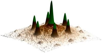
A residual interaction with the SiC substrate causes the formation of the six-fold satellite reflex structure.
Christoph Tegenkamp, Leibniz Universität Hannover
The structure of graphene itself is fascinating: It consists of exactly one single, regular layer of carbon atoms. To manufacture this incredibly thin layer absolutely neatly is a great challenge. A possible method to recipitate graphene extensively on an insulating substrate is epitaxy, i.e. the controlled growth of graphene on insulating silicon carbide. For this purpose, a silicon carbide crystal is heated in vacuum. Starting from a specific temperature, carbon atoms migrate to the surface and form a monoatomic layer on the - still solid - silicon carbide. An important question for later applications is, how defects and steps of the silicon carbide surface affect the electronic properties of the graphene grown on it.
Within the scope of a research cooperation between PTB and Leibniz University Hanover, the influence of defects in the graphene on the electronic properties has been investigated. During the investigations, special attention was paid to the influence of the defects on a special electronic excitation, the so-called plasmons.
By different sample preparation, first of all silicon carbide crystals with different surface roughness and, thus, with a different concentration of surface defects were investigated, on which, subsequently, graphene formed. The influence of the defects on the plasmon excitations was then investigated by means of low-energy electron diffraction (SPA-LEED) and electron loss spectroscopy (EELS).
The process revealed a strong dependence of the lifetime of plasmon on the surface quality. Defects, as they are caused on step edges and grain boundaries, strongly impede the propagation of the plasmons and drastically shorten their lifetime. Here it is remarkable that the other electronic properties of the plasmons, in particular their dispersion, remain largely unaffected.
This opens up interesting possibilities for the future technical application and use of plasmons (the so-called "plasmonics") in graphene. By selective adjustment of the surface roughness, different graphene ranges could be generated in which the plasmons are either strongly dampened or can propagate almost unobstructedly. In this way, the plasmons could be conducted along "plasmon conductors" with low surface roughness specifically from one point of a graphene chip to another.
Original publication: T. Langer, J. Baringhaus, H. Pfnür, H. W. Schumacher and C. Tegenkamp; "Plasmon damping below the Landau regime: the role of defects in epitaxial graphene"; New Journal of Physics 12, 033017 (2010)
See the theme worlds for related content
Topic World Spectroscopy
Investigation with spectroscopy gives us unique insights into the composition and structure of materials. From UV-Vis spectroscopy to infrared and Raman spectroscopy to fluorescence and atomic absorption spectroscopy, spectroscopy offers us a wide range of analytical techniques to precisely characterize substances. Immerse yourself in the fascinating world of spectroscopy!


