When plasmons reach atomic flatland
Potential implications for novel imaging techniques and photochemical reactions at the nanoscale
Researchers from the Max Planck Institute for the Structure and Dynamics of Matter in Hamburg, Germany, and the Lawrence Berkeley National Laboratory (LBNL) in the United States have discovered a significant new fundamental kind of quantum electronic oscillations, or plasmons, in atomically thin materials. Their work has now been published in Nature Communications. It has potential implications for novel imaging techniques and photochemical reactions at the nanoscale.

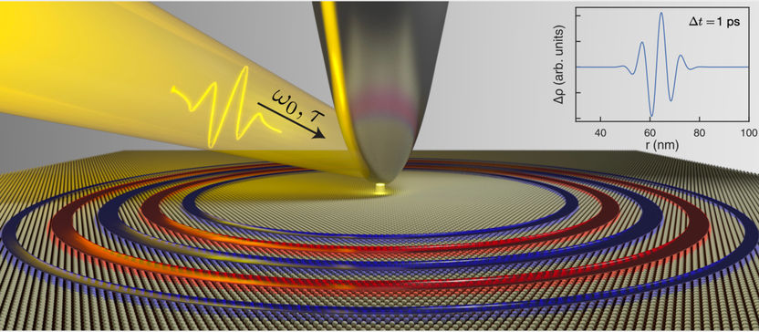
Snapshot of a calculation showing a slowly moving plasmon wave packet excited on monolayer TaS2. The plasmon wave packet is highly localized in real space even at
© Felipe da Jornada
Almost seventy years ago, scientists showed that electrons in materials could sustain wavelike propagating oscillations, known as plasmons. Nowadays, there is a vibrant field of plasmonics which studies these electronic oscillations, with applications such as faster computer chips, solar cells, biosensors, and even cancer treatments.
Plasmons are strongly affected by the geometry of their host materials, which makes them very tunable for different applications. However, it was not clear how plasmons behave in an extreme case: when materials are just a couple of atoms thick.
The international research team consisting of Felipe da Jornada and Steven Louie from the LBNL at the University of California, Berkeley, and Lede Xian and Ángel Rubio from the MPSD, which is based at the Center for Free-Electron Laser Science (CFEL), wanted to shed new light on the properties of plasmons in these novel atomically thin materials.
Using parameter-free quantum calculations, they found that plasmons behave in a peculiar way in all atomically thin materials. This was initially a surprise to the authors: “Textbook physics says that plasmons in bulk materials behave in one way, and in strictly two-dimensional materials, in another way. But unlike these simplified models, plasmons in all real, atomically thin materials behave yet differently and tend to be much more localizable in space,” says Felipe Jornada, who is now based at Stanford University.
The reason for this difference, Steven Louie argues, is that “in real atomically thin materials, all the other electrons that are not conducting and oscillating can screen these plasmons, which leads to a fundamentally different dispersion relations for these excitations.”
Other key findings of their research are that the plasmons in systems such as monolayer TaS2 can remain stable for long times (~ 2 ps) and are virtually dispersionless for wavevectors which are commonly used in certain experiments. This indicates that plasmons in atomically thin materials are localizable in real space with available experimental techniques and could significantly enhance the intensity of light by a factor of more than 10⁷.
Ángel Rubio, the director of the MPSD’s Theory Department, says: “These findings are relevant for many applications, from promoting photocatalytic reactions to biosensing and single-molecule spectroscopy.”
Original publication
Other news from the department science

Get the chemical industry in your inbox
By submitting this form you agree that LUMITOS AG will send you the newsletter(s) selected above by email. Your data will not be passed on to third parties. Your data will be stored and processed in accordance with our data protection regulations. LUMITOS may contact you by email for the purpose of advertising or market and opinion surveys. You can revoke your consent at any time without giving reasons to LUMITOS AG, Ernst-Augustin-Str. 2, 12489 Berlin, Germany or by e-mail at revoke@lumitos.com with effect for the future. In addition, each email contains a link to unsubscribe from the corresponding newsletter.


