A fast light detector made of two-dimensional materials
Technology with multiple possibilities
Advertisement
Two research groups at ETH Zurich have joined forces to develop a novel light detector. It consists of two-dimensional layers of different materials that are coupled to a silicon optical waveguide. In the future, this approach can also be used to make LEDs and optical modulators.
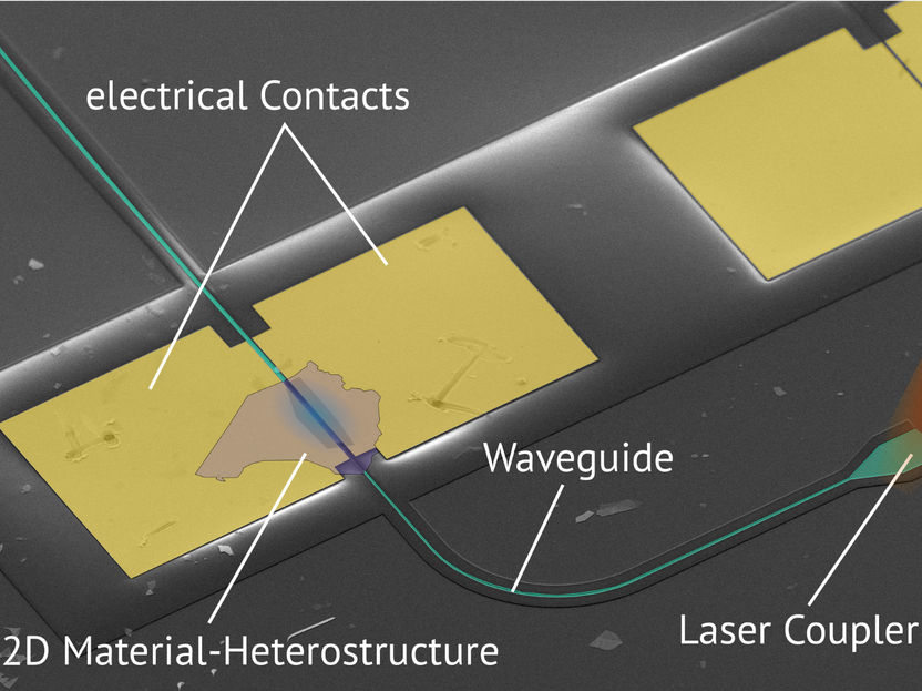
An electron microscope image of the ETH light detector with the thin layer of the two-dimensional heterostructure, the optical waveguide and the electrical contacts through which the signal of the detector is read out.
ETH Zürich
Fast and highly efficient modulators as well as detectors for light are the core components of data transmission through fibre optic cables. In recent years, those building blocks for telecommunications based on existing optical materials have been constantly improved, but now it is getting increasingly difficult to achieve further improvements. That takes the combined forces of different specializations, as two research groups at ETH Zurich have now shown.
A group of scientists led by professors Jürg Leuthold of the Institute for Electromagnetic Fields and Lukas Novotny of the Institute for Photonics, together with colleagues at the National Institute for Material Science in Tsukuba (Japan), have developed an extremely fast and sensitive light detector based on the interplay between novel two-dimensional materials and nano-photonic optical waveguides.
Two-dimensional materials
“In our detector we wanted to exploit the advantages of different materials whilst overcoming their individual constraints,” explains Nikolaus Flöry, a PhD student in Novotny’s group. “The best way of doing so is to fabricate a kind of artificial crystal – also known as heterostructure – from different layers that are each only a few atoms thick. Moreover, we were interested to know whether all the buzz about such two-dimensional materials for practical applications is actually justified.”
In two-dimensional materials, such as graphene, electrons only move in a plane rather than three spatial dimensions. This profoundly alters their transport properties, for instance when an electrical voltage is applied. While graphene is not the ideal choice for optics applications, compounds of transition metals such as molybdenum or tungsten and chalcogenes such as sulphur or tellurium (abbreviated as TMDC) are highly photosensitive and, on top of that, can be easily combined with silicon optical waveguides.
Interplay of different approaches
The expertise for the waveguides and high-speed optoelectronics came from the research group of Jürg Leuthold. Ping Ma, the group’s Senior Scientist, stresses that it was the interplay between the two approaches that made the new detector possible: “Understanding both the two-dimensional materials and the waveguides through which light is fed into the detector was of fundamental importance to our success. Together, we realized that two-dimensional materials are particularly suited to being combined with silicon waveguides. Our groups’ specializations complemented each other perfectly.”
The researchers had to find a way to make the ordinarily rather slow TMDC-based detectors faster. On the other hand, the detector had to be optimally coupled to the silicon structures used as an interface without sacrificing its high-speed performance.
Speed through vertical structure
“We solved the speed problem by realizing a vertical heterostructure made of a TMDC – molybdenum ditelluride in our case – and graphene,” Flöry says. Differently from conventional detectors, in that way electrons excited by incoming light particles don’t need to first make their way through the bulk of the material before being measured. Instead, the two-dimensional layer of TMDC ensures that electrons can leave the material in a very short time either upwards or downwards.
The faster they leave, the larger is the bandwidth of the detector. The bandwidth indicates at what frequency data encoded in light pulses can be received. “We had hoped to get a few Gigahertz of bandwidth with our new technology – in the end, we actually reached 50 Gigahertz,” says Flöry. Up to now, bandwidths of less than a Gigahertz were possible with TMDC-based detectors.
Optimal light coupling, on the other hand, was achieved by integrating the detector into a nano-photonic optical waveguide. A so-called evanescent wave, which laterally protrudes from the waveguide, feeds the photons through a graphene layer (which has a low electrical resistance) into the molybdenum-ditelluride layer of the heterostructure.
There, they excite electrons that are eventually detected as a current. The integrated waveguide design ensures that enough light is absorbed in that process.
Technology with multiple possibilities
The ETH researchers are convinced that with this combination of waveguides and heterostructures they can make not just light detectors, but also other optical elements such as light modulators, LEDs and lasers. “The possibilities are almost limitless,” Flöry and Ma enthuse about their discovery. “We just picked out the photodetector as an example of what can be done with this technology.”
In the near future, the scientists want to use their findings and investigate other two-dimensional materials. About a hundred of them are known to date, which gives countless possible combinations for novel heterostructures. Moreover, they want to exploit other physical effects, such as plasmons, in order to improve the performance of their device even further.


