Imprinted Color Patterns
Azopolymer material allows light-assisted imprinting of nanostructures for structurally colored surfaces
structural colors appear because the imprinted pattern on a surface changes the wavelengths of light. Chinese scientists have introduced an azopolymer that allows the imprinting of nanopatterns in a novel room-temperature lithographic process. A key aspect of the technique is the light-induced phase change of a novel azopolymer, explains the study published in the journal Angewandte Chemie. The process relies solely on light regulation and allows nanoimprinting even on flexible substrates.
© Wiley-VCH
Delicately structured surfaces are present in many relevant areas, including anticounterfeiting of banknotes and chip manufacturing. In the electronics industry, surface patterns, such as printed circuits, are created by photolithographic processes. Photolithography means that a photoresist, a polymeric material sensitive to ultraviolet (UV) light, is irradiated through a mask. The weakened areas are washed away, and the structures are finished by etching, imprinting, and other processes. To prepare the photoresist for UV-light irradiation, heating and cooling are important steps, which cause changes in the material behavior.
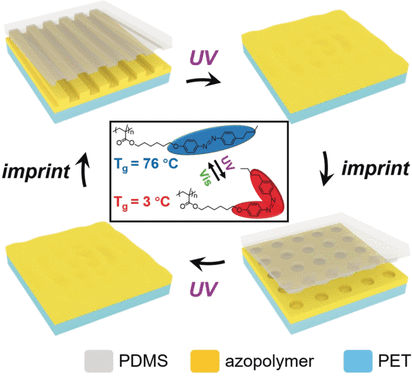
Unfortunately, materials tend to shrink upon cooling, which poses problems when nanosized patterns are desired. Therefore, Haifeng Yu and his colleagues from Peking University have developed a nanolithography process that works entirely at room temperature. Key to the method is a novel photoresist that changes its mechanical behavior solely by light irradiation. A heating step is no longer necessary. The new photoresist contains a chemical component called azobenzene, which switches from a straight “trans” into a bent “cis” form, and vice versa, when irradiated with light. This azobenzene, which is attached to the polymer backbone, causes the mechanochemical changes of the resulting azopolymer.
For pattern fabrication, the authors first liquefied the azopolymer layer coated on a flexible plastic surface by shining UV light on it. Then they pressed a transparent nanopatterned silicone sheet on the liquefied areas and irradiated the layers with visible light. This light induced hardening of the azopolymer, which adopted the template nanopattern. Then the scientists applied a photomask and irradiated the layers with UV light to re-liquefy the uncovered areas. For the final imprint, they pressed another nanopatterned sheet on the azopolymer structure and hardened the layers with visible light to obtain the finished nanopatterned coating layer. This technique is called “athermal nanoimprint lithography”.
The nanopatterned surface appeared in multiple structural colors. Tiny letters or ornamental drawings changed their colors depending on the angle they were viewed at. According to the authors, the technique is not limited to structural colors. “It is adaptable to many other substrates like silicon wafers and other light-active materials,” they say. The researchers envision applications in nanofabrication areas where heat-independent imprinting processes are required and phototunable materials have advantages.
Original publication
Other news from the department science

Get the chemical industry in your inbox
By submitting this form you agree that LUMITOS AG will send you the newsletter(s) selected above by email. Your data will not be passed on to third parties. Your data will be stored and processed in accordance with our data protection regulations. LUMITOS may contact you by email for the purpose of advertising or market and opinion surveys. You can revoke your consent at any time without giving reasons to LUMITOS AG, Ernst-Augustin-Str. 2, 12489 Berlin, Germany or by e-mail at revoke@lumitos.com with effect for the future. In addition, each email contains a link to unsubscribe from the corresponding newsletter.
Most read news
More news from our other portals
Last viewed contents
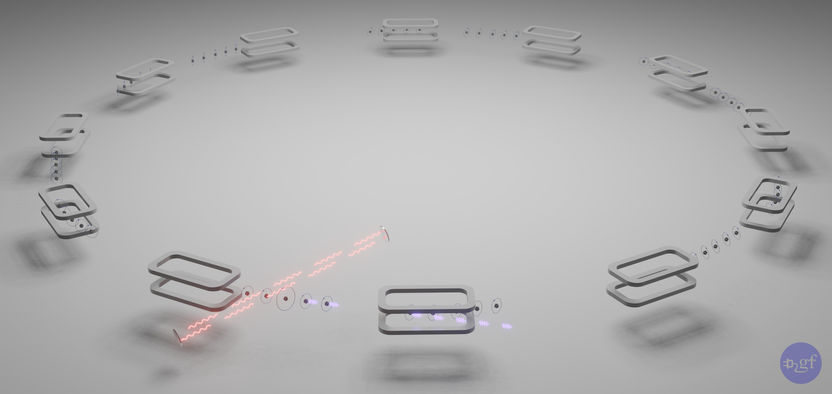
New ‘super light source’ should allow fascinating insights into atoms - ‘Gamma Factory’ will enable not only breakthroughs in spectroscopy but also novel ways of testing fundamental symmetries of nature
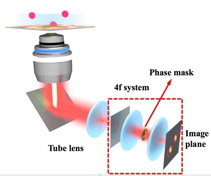
Shaping light lets 2D microscopes capture 4D data - Invention adds new dimension to fluorescent microscopy
3D Hierarchically Porous Nanostructured Catalyst Helps Efficiently Reduce CO2
Biological_small-angle_X-ray_scattering
Luminiferous_aether
Micromeritics Instrument Corp. acquires Freeman Technology
Self-envy
Physicists propose a new method for monitoring nuclear waste - Scenarios for using neutrino detectors in nuclear interim storage facilities
Green_infrastructure
Stephen_Hanessian
Redox
