Researchers develop new 3D printing for the direct production of nanostructures
Advertisement
A team from Graz University of Technology succeeded in using the FEBID method to produce complex 3D-printed nano-components for the first time without additional support structures.
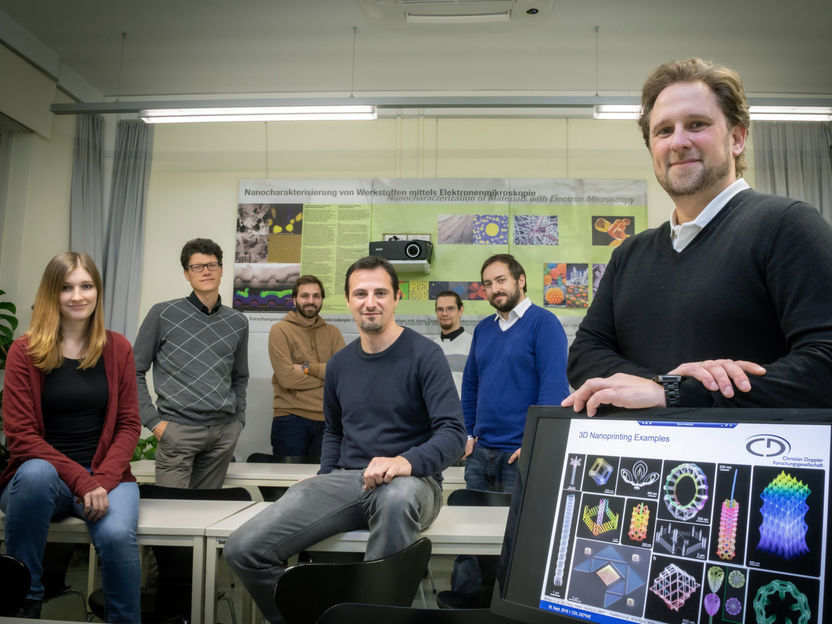
The successful team of the Christian Doppler Laboratory for Direct Write Fabrication of 3D Nano-Probes (from left to right): Anna Weitzer, David Kuhness, Lukas Seewald, Robert Winkler, Jürgen Sattelkow, Jakob Hinum-Wagner and Harald Plank.
© Lunghammer – TU Graz
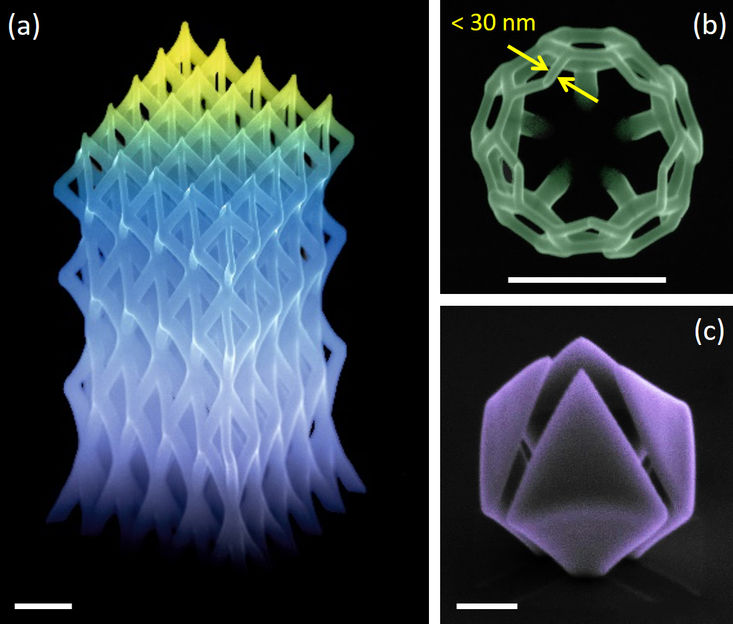
Examples from the three-dimensional printed nanoworld show the complexity (a), the achievable structure sizes (b) as well as the path from meshed towards closed 3D surfaces (c). All images are re-coloured scanning electron microscope micrographs with a 500 nm wide scale bar.
© Harald Plank, Institut für Elektronenmikroskopie und Nanoanalytik der TU Graz

In the nanometer range, complex, free-standing 3D architectures are very difficult to produce in a single step due to the required precision. In the Christian Doppler Laboratory for Direct Write Fabrication of 3D Nano-Probes, scientists at Graz University of Technology are therefore devoting themselves to the fundamentals of 3D Nanoprinting to push its possibilities beyond current limitations. For that, the research group uses the technology Focused Electron Beam Induced Deposition (FEBID), which is already used successfully in the production of complex but often flat nanostructures.
More efficiency and more possibilities
The CD lab research team has advanced the technology in such a way, that even complex three-dimensional nanostructures can be produced in a highly controlled and predictable way. In addition to the production of new structures, the process also enables the modification of already finished micro and nano components. The individual, nanometer thin layers, which finally form the 3D architectures, adhere to virtually any material and surface morphology. That saves time because FEBID does not require any pre- or post-treatment of the samples. On the other hand, it also enables fabrication on uneven or rough surfaces. "This type of 3D nanoprinting opens up completely new playgrounds for science and industry," says Harald Plank from the Institute of Electron Microscopy and Nanoanalysis at TU Graz and head of the CD lab. With the new technology, future challenges can be mastered that are barely possible with alternative nanofabrication methods such as electron beam lithography. "With this method, it would also be possible to produce 3D nanostructures on a pencil tip in a single step, which is very difficult to do with alternative technologies," explains Plank.
How the new 3D nanoprinting technology works
The new process will be used in cooperation with industrial partners GETec Microscopy (Vienna) and Anton Paar GmbH (Graz) in the field of atomic force microscopy for the production of functional nano-probes with apex radii of less than ten nanometers. "The printing process takes place in the vacuum chamber of electron microscopes. The functional gases are introduced with a fine capillary in close proximity to the sample. The gaseous molecules then adsorb on the surface and are chemically broken down and immobilised by the focused electron beam – they remain in place through interaction with the electrons," explains Plank. "You can imagine 3D nanoprinting like a ballpoint pen: The electron beam acts like a ballpoint pen refill and the gas is the ink."
Plank and his team were inspired by Lego bricks for printing inclined structures: "To build a tilted architecture using Lego, the next higher layer of bricks must always be moved sideward. This is exactly what we have transferred to 3D nanoprinting: Before applying the next layer, we shift the electron beam and literally print diagonally upwards."
Successful implementation
During the last 20 months, the CD lab was able to deliver the first proof-of-principle. In more detail, FEBID was successfully used for the production of electrically conductive nanoprobes, whose performance is significantly higher than that of alternative, commercially available products. Plank and his team are satisfied with the result: "Small series production will start in Vienna in the coming months and open up new possibilities for the industrial partner GETec Microscopy.”
International cooperation
To ensure that the new process does not remain a niche technology, the researchers in the CD lab are currently developing a new software for FEBID based 3D Nanoprinting, which will allow fabrication of complex nanostructures even without broad prior knowledge. For that, Plank and his research group have joined forces with Oak Ridge National Laboratories (USA) and the Institute of Physics at the Goethe University Frankfurt (GER), which together with Graz University of Technology are among the world's leading research institutions in this field. This project also focuses on extending the process to 3D surfaces and multi-material structures, which further increases the design flexibility and thus the relevance of this technology in research and development.


