How to design efficient materials for OLED displays
For applications such as light-emitting diodes or solar cells, organic materials are nowadays in the focus of research. These organic molecules could be a promising alternative to currently used semiconductors such as silicon or germanium and are used in OLED displays. A major problem is that in many organic semiconductors the flow of electricity is hampered by microscopic defects. Scientists around Dr. Gert-Jan Wetzelaer and Dr. Denis Andrienko of the Max-Planck-Institute for Polymer Research have now investigated how organic semiconductors can be designed such that the electric conduction is not influenced by these defects.

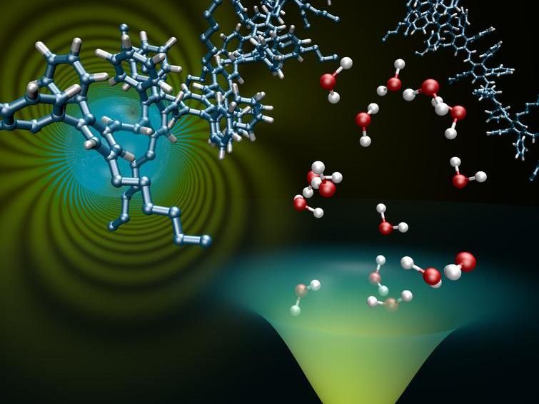
Charges in organic semiconductors can be trapped by either oxygen or water molecules
© D. Andrienko / MPI-P
The basic principle of the first light bulb, invented by Thomas Edison in the 19th century, was quite simple: Electrons – negatively charged particles – flow through a carbon filament and create light by converting their energy to light and heat. Nowadays, the physics of the generation of light in semiconducting devices is more complex: Electrons flow through a device and release their energy at a given point in the device. For this, they have to find a free place, i. e. a place that isn’t occupied by an electron - at a deeper lying energy level. This free place can be viewed as a sort of positive charge, a so called hole. If the electron jumps down into the hole, its energy is released in the form of light. Based on this principle, an organic light-emitting diode (OLED) converts electric current into light.
The efficiency of such a device strongly depends on how good holes and electrons can be conducted. If either electrons or holes are trapped by defects, meaning that they cannot contribute to the current anymore, then an excess of one type of charge exists. For example, in the case that holes are trapped, there are more electrons than holes, meaning only a part of the electrons can create light and the efficiency of the OLED is reduced.
“In our newest experiments, we examined a large range of organic semiconductors and found out the main parameters that are essential for equal and defect-free conduction of both holes and electrons”, says Gert-Jan Wetzelaer (Department of Prof. Paul Blom). In a semiconductor, electrons are moving at a higher energy level, whereas holes move at a level lower (deeper) in energy. The scientists found that the conduction of both charge types strongly depends on the position of these energy levels. “Depending on the energy of these levels the charge transport can be dominated either by electrons or holes or, with the right choice of energy levels, they contribute equally to the charge transport,” says Wetzelaer.
In computer simulations, scientists around Denis Andrienko (Department of Prof. Kurt Kremer) had a deeper look at the origin of these charge traps: “In our simulations we introduced clusters of water molecules in the semiconductor, which may accumulate in little pockets in the semiconductor”, explains Andrienko. “We found that these clusters of water molecules can function as a hole trap, leading to electron-dominated organic semiconductors. By contrast, for hole-dominated semiconductors, oxygen related defects capture electrons. As a result, we could show that highly unipolar charge transport for either holes or electrons is governed by a very small amount of defects, such as water and oxygen.” Unfortunately, removing such defects completely has proven challenging.
Therefore, the Mainz researchers are able to define how to design highly efficient organic semiconductors in the future: The different energy levels of the material should be in a certain range, which strongly reduces the influence of oxygen and water molecules that are the main cause for charge trapping. Based on this concept, the first highly efficient OLEDs with defect-free electrical conduction have recently been realized.
Original publication
Other news from the department science

Get the chemical industry in your inbox
By submitting this form you agree that LUMITOS AG will send you the newsletter(s) selected above by email. Your data will not be passed on to third parties. Your data will be stored and processed in accordance with our data protection regulations. LUMITOS may contact you by email for the purpose of advertising or market and opinion surveys. You can revoke your consent at any time without giving reasons to LUMITOS AG, Ernst-Augustin-Str. 2, 12489 Berlin, Germany or by e-mail at revoke@lumitos.com with effect for the future. In addition, each email contains a link to unsubscribe from the corresponding newsletter.


