Silicon as a semiconductor: silicon carbide would be much more efficient
In power electronics, semiconductors are based on the element silicon – but the energy efficiency of silicon carbide would be much higher. Physicists of the University of Basel, the Paul Scherrer Institute and ABB explain what exactly is preventing the use of this combination of silicon and carbon in the scientific journal Applied Physics Letters.

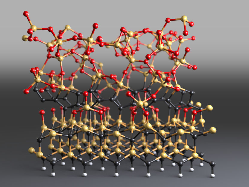
At the interface between silicon dioxide and silicon carbide, irregular clusters of carbon rings occur, which disturb the electronic function.
University of Basel, Departement Physik/Swiss Nanoscience Institute
Energy consumption is growing across the globe; electric power is being relied upon more and more, and sustainable energy supplies such as wind and solar power are becoming increasingly important. Electric power, however, is often generated a long distance away from the consumer. Efficient distribution and transport systems are thus just as crucial as transformer stations and power converters that turn the generated direct current into alternating current.
Huge savings are possible
Modern power electronics must be able to handle large currents and high voltages. Current transistors made of semiconductor materials for field-effect transistors are now mainly based on silicon technology. Significant physical and chemical advantages, however, arise from the use of SiC over silicon: in addition to a much higher heat resistance, this material provides significantly better energy efficiency, which could lead to massive savings.
It is known that these advantages are significantly compromised by defects at the interface between silicon carbide and the insulating material silicon dioxide. This damage is based on tiny, irregular clusters of carbon rings bound in the crystal lattice, as experimentally demonstrated by researchers led by Professor Thomas Jung at the Swiss Nanoscience Institute and Department of Physics from the University of Basel and the Paul Scherrer Institute. Using atomic force microscope analysis and Raman spectroscopy, they showed that the defects are generated in the vicinity of the interface by the oxidation process.
Experimentally confirmed
The interfering carbon clusters, which are only a few nanometers in size, are formed during the oxidation process of silicon carbide to silicon dioxide under high temperatures. “If we change certain parameters during oxidation, we can influence the occurrence of the defects,” says doctoral student Dipanwita Dutta. For example, a nitrous oxide atmosphere in the heating process leads to significantly fewer carbon clusters.
The experimental results were confirmed by the team led by Professor Stefan Gödecker (Department of Physics and Swiss Nanoscience Institute, University of Basel). Computer simulations confirmed the structural and chemical changes induced by graphitic carbon atoms as observed experimentally. Beyond experiments, atomistic insight has been gained in the generation of the defects and their impact on the electron flow in the semiconductor material.
Better use of electricity
“Our studies provide important insight to drive the onward development of field-effect transistors based on silicon carbide. Therefore we expect to provide a significant contribution to the more effective use of electrical power,” comments Jung. The work was initiated as part of the Nano Argovia program for applied research projects.
Original publication
D. Dutta, D. S. De, D. Fan, S. Roy, G. Alfieri, M. Camarda, M. Amsler, J. Lehmann, H. Bartolf, S. Goedecker, T. A. Jung; "Evidence for carbon clusters present near thermal gate oxides affecting the electronic band structure in SiC-MOSFET"; Applied Physics Letters; 2019
Original publication
D. Dutta, D. S. De, D. Fan, S. Roy, G. Alfieri, M. Camarda, M. Amsler, J. Lehmann, H. Bartolf, S. Goedecker, T. A. Jung; "Evidence for carbon clusters present near thermal gate oxides affecting the electronic band structure in SiC-MOSFET"; Applied Physics Letters; 2019
Organizations
Other news from the department science

Get the chemical industry in your inbox
By submitting this form you agree that LUMITOS AG will send you the newsletter(s) selected above by email. Your data will not be passed on to third parties. Your data will be stored and processed in accordance with our data protection regulations. LUMITOS may contact you by email for the purpose of advertising or market and opinion surveys. You can revoke your consent at any time without giving reasons to LUMITOS AG, Ernst-Augustin-Str. 2, 12489 Berlin, Germany or by e-mail at revoke@lumitos.com with effect for the future. In addition, each email contains a link to unsubscribe from the corresponding newsletter.


