Laser technology supports the path to printed electronic diversity
In recent years, the demands placed on component-integrated electronics have risen so sharply in many industries that they can often no longer be met with conventional electronic components. As an alternative, printed electronics is on the advance. At the Hanover Fair from April 1 to 5, 2019, experts from the Fraunhofer Institute for Laser Technology ILT in Aachen, Germany, will be demonstrating the role lasers play in this process. Highlights include the directly printed strain gauge sensor, the locally gold-plated contacts and the electrically conductive glass fiber fabric.
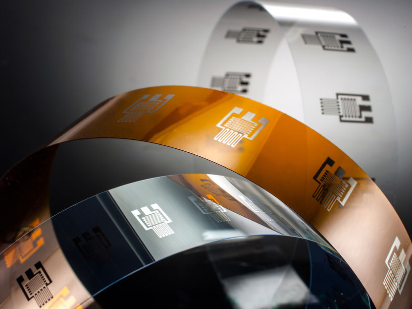
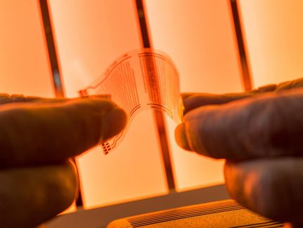
Direct printing: Fraunhofer ILT is demonstrating a strain gauge sensor that can be applied directly and automatically to the component thanks to a combination of printing and laser technology.
Fraunhofer ILT, Aachen
Fraunhofer ILT's Thin Film Processing group specializes in the post-treatment of coatings using lasers: One of its focal points is the laser-based treatment of printed, thin electronic layers. Wet coating processes such as inkjet, pad or dispensing printing and many others are used to deposit the necessary materials onto the components to integrate electrical functions into them. Depending on the process, different layers can be applied which vary in thickness, width or structure.
Laser-based heat post-treatment in two steps
However, all layers have a common denominator: They require heat post-treatment, which is carried out conventionally in a furnace, for example. "The post-treatment using furnaces can take a long time and is very energy-intensive because the entire component is heated," explains Dr. Christian Vedder, group leader at Fraunhofer ILT. "In its place, a laser beam can be used, which works much more precisely and quickly: It can process small structures on components in such a short time that the coating can be heated locally to temperatures above the damage threshold of the component, but without damaging the component itself. Laser processing takes place in two steps: First, the laser beam dries the layer to remove solvents. As a result, only the functional particles, for example silver, gold, etc., remain. The laser then partially or completely melts these micro- or nanoparticles and connects them so that they can conduct electricity, for example.
Printed sensor replaces strain gauges
Fraunhofer ILT is demonstrating its capabilities in this field, for example, with an additively manufactured strain gauge that can be used to measure the elongation of a component. The Aachen researchers have developed a method for directly applying the sensor to substitute the conventional foil strain gauge, which commonly has to be applied manually to the component. To achieve this, the scientists deposit an insulation layer on a metallic component, onto which a measuring grid including conductor paths is printed by means of inkjet or aerosol jet. All post-treatment is done using laser radiation. If necessary, a final encapsulation with a further insulation layer follows. "We will be presenting the design and functionality of a demonstrator in Hanover," says Dr. Vedder. "We show how the electrical resistance of the additive measuring grid changes under mechanical stress. In addition, we’ll be presenting a variety of different geometries."
Individual car doors enabled by process combination
Results of the Fraunhofer lighthouse project »Go Beyond 4.0« will also be displayed: The Fraunhofer Institutes ENAS, IFAM, IWU, ISC, IOF and ILT are working on the application of electronic functional layers on components from the automotive, aviation and lighting sectors. These development activities are particularly interesting for vehicle manufacturers who install a great deal of electronics in cars and trucks – ranging from the windscreen wiper control over the camera module in the bumper all the way to modern sensors. "With the new technology, it will be possible to individualize mass components, such as doors, using digital print and laser processes. In the future, electrical signal and power interconnects for different car configurations may be applied directly and automatically to the components, without having to keep individual cable harnesses available," said the ILT scientist assessing the potential of this technology. In addition to printing electrical conductors, this technology enables the integration of new sensors and lighting elements. "We are starting with surface structuring using laser ablation: Cavities of almost any shape can be manufactured which will then be coated with an electrical insulation layer using digital printing technologies. The laser post-treatment of the insulation layer is followed by printing another layer of electrical conductors or sensors and their laser-based post-treatment.
Ready for take-off: A multi-functional aircraft wing
Within the lighthouse project »Go Beyond 4.0«, a demonstrator part for the aerospace industry will also be developed. Carbon or glass fiber fabrics are in demand due to the need for weight reduction. Using a combination of printing and laser technology, the researchers can apply electrical functional layers directly to the fabrics, which then are embedded into the component matrix material. The functional elements are thus protected in the fiber composite component. In addition to electrical interconnects for new sensors and lighting elements, heating structures in aircraft wings, for example, could also be manufactured in this way.
Waste passé: Local gold-plating of electrical contacts
In Hanover, the Fraunhofer ILT will display further applications for the combination of printing and laser technology. One approach demonstrates how plug contacts can be gold-plated more selectively than before: The gold is only applied at spots where the electrically conductive contact is actually required. The approach boasts many advantages: Not only does the process reduce the amount of gold needed – compared to a fully gold-plated part – but it has a design flexibility and independence from long delivery times that plague the industry.
Battery manufacturers might be interested in a laser-based method for drying battery electrode layers that are prior deposited as pastes to copper foils. This method saves both energy and installation space, two more advantages.
Fraunhofer ILT also uses laser radiation to create functional layers for microelectronic accelerometers. A piezoelectric actuator, however, is used to generate motion: It deforms when voltage is applied. Here, the Aachen researchers are investigating how the piezoelectric layers can be applied in a more cost-saving way using laser radiation for crystallization.
