Semiconductors: No support needed
Scientists at LMU are the first to fabricate freely suspended, ultrathin, organic semiconductor films
In recent years, interest in the investigation of several organic semiconductor materials has steadily increased. These compounds promise easier and cheaper fabrication without the need for scarce elements, as well very favorable electrical switching characteristics and correspondingly high performance. They are also amenable to large-scale production techniques, including printing processes. Their inherent properties, such as their flexibility, are compatible with applications in new electronic devices, such as displays and sensors.
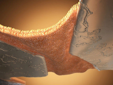
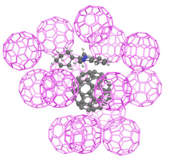
Artists view of freely suspended organic semiconductor thin film (selected front cover in Advanced Materials).
C. Hohmann (Nanosystems Initiative Munich, NIM)
Up to now, precise characterization of the properties of these materials has been difficult. This is in part because organic semiconductors have so far been mounted on top of a supporting substrate. The substrate, as well as the resulting interfaces, inevitably have an impact on, for example, chargecarrier mobility, and could therefore influence and distort the natural processes inherent to the material.
Focusing on this issue, Professor Thomas Weitz and Professor Achim Hartschuh have developed a way to fabricate freely suspended, ultrathin, organic semiconductor films.
Only two semiconducting layers
In their experiments, the physicists were able to fabricate organic semiconducting films consisting of only two to three layers of material but spanning several hundreds of nanometers (channel lengths of 100-450 nm and widths of 0.5-1 µm) without a supporting substrate.
In contrast to inorganic semiconductors, the crystal structure of their organic counterparts is stabilized by van der Waals forces. Such bonds are at least two orders of magnitude weaker than covalent bonds. “Nevertheless, our measurements indicate that our suspended semiconductor thin films exhibit high crystal quality,” stresses Thomas Weitz, “and the material has excellent stability and electrical properties.”
Freely suspended and electronically decoupled films
The aim of the project was to synthesize highly ordered and electronically active organic films, which are as thin as possible and are completely isolated from their environment. Temperature-dependent charge-transport measurements confirmed that the suspended films were indeed electrically decoupled.
Up to now, freely suspended, few-nm-thin semiconductor films with purely van der Waals bond-mediated stability have not been realized and hence could not be studied. Those now described by Weitz and colleagues are the first of their kind, and will permit detailed study of the charge transport processes in such films.
Original publication
Other news from the department science

Get the chemical industry in your inbox
By submitting this form you agree that LUMITOS AG will send you the newsletter(s) selected above by email. Your data will not be passed on to third parties. Your data will be stored and processed in accordance with our data protection regulations. LUMITOS may contact you by email for the purpose of advertising or market and opinion surveys. You can revoke your consent at any time without giving reasons to LUMITOS AG, Ernst-Augustin-Str. 2, 12489 Berlin, Germany or by e-mail at revoke@lumitos.com with effect for the future. In addition, each email contains a link to unsubscribe from the corresponding newsletter.
Most read news
More news from our other portals
Last viewed contents
Category:Flavin_enzymes

Blow flies can be used to detect use of chemical weapons, other pollutants - Using mass spectrometry to determine the chemicals in the blow flies' guts
How safe is graphene? - Effects on people and the environment under the microscope
Largest Synthetic Polysaccharide Assembled - Linear 100-mer polysaccharide within 188 hours
Microwave_oven
Category:Indicator_species
Advanced X-ray technique unveils fast solid-gas chemical reaction pathways
Hydrogen march! The Energy Carrier of the Future is Obtained at LIKAT from a Simple Ester - Unexpectedly powerful start
