Tandem Solar Cells – Record Efficiency for Silicon-based Multi-junction Solar Cell
silicon solar cells dominate the photovoltaic market today but the technology approaches the theoretical maximum efficiency that can be achieved with silicon as the only absorber material. tandem solar cells, on the other hand, combine several absorber materials, enabling a better energetic use of the solar irradiance spectrum. Due to their higher efficiency potential, tandem solar cells have a promising future. After intensive research, scientists at Fraunhofer ISE in cooperation with partners have achieved a new efficiency record of 22.3 percent for a multi-junction solar cell made of silicon and III-V semiconductor materials. The outstanding achievement is that the III-V layers were directly grown on the silicon.

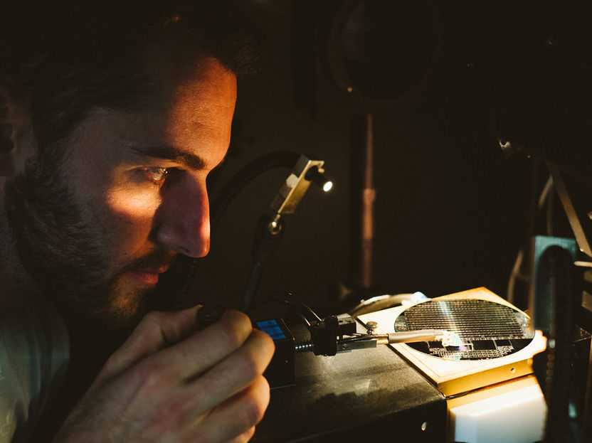
With the tandem solar cell made of silicon and III-V semiconductor materials, a more energetically efficient use of the solar spectrum is possible, compared to conventional solar cells available today.
© Fraunhofer ISE/A.Wekkeli
Combining the Best Materials
By combining different semiconductor materials, solar cell researchers are attempting to surpass the theoretical efficiency limit of 29.4 percent for a single-junction silicon solar cell, and convert sunlight into electricity even more efficiently. Promising is the combination of silicon material with III-V semiconductor compounds like gallium arsenide. To realize this, one approach is to first deposit the III-V solar cell structures on gallium arsenide substrates, then transfer to a silicon solar cell using semiconductor bonding technology and lastly etch away the gallium-arsenide substrate. Another less costly approach, however, is to directly grow the III-V layers on the silicon solar cell. In this second approach, the atomic structure must be controlled extremely well during growth so that the gallium and phosphorous atoms arrange on the correct lattice sites at the interface to the silicon material. Also, the distance between the atoms in the crystal lattice must be increased in order to produce the gallium arsenide material. Researchers have been working on these challenges for over ten years. Now they have been able to greatly reduce the defect density in the III-V semiconductor layers on the silicon and have successfully produced a III-V/Si tandem solar cell with a new efficiency record of 22.3 percent using this direct-growth approach. The efficiency value was published in the internationally recognized table of the best research-cell efficiencies worldwide on December 25, 2018.
“We are delighted with this result for the direct growth of III-V semiconductors on silicon, an important research approach for tandem solar cells,” says Dr. Andreas Bett, institute director of Fraunhofer ISE. “In Freiburg, we are presently building a new research center for high efficiency solar cells. Our work on tandem cells will be carried out in the new facilities upon its completion in 2020. With the improved technical infrastructure, we expect the developments in multi-junction solar cells based on silicon to accelerate rapidly.”
Within the MehrSi project over the past years, the junction between the silicon crystal and the first III-V semiconductor layer of gallium phosphide was investigated and continuously optimized in close cooperation with the research groups of Prof. Thomas Hannappel on the TU Ilmenau and of Prof. Kerstin Volz at the Philipps University Marburg. The defects in the crystalline structure were first made visible and then reduced step by step. “The record efficiency of our III-V/Si tandem solar cell demonstrates that we have achieved a very good understanding of the materials,” explains Dr. Frank Dimroth, coordinator of the MehrSi project. With the successful direct growth of III-V layers on silicon, we can avoid using expensive III-V substrates for epitaxy. This approach is, therefore, a key technology for the cost-effective manufacture of high efficiency tandem solar cells in the future.
Other news from the department science

Get the chemical industry in your inbox
By submitting this form you agree that LUMITOS AG will send you the newsletter(s) selected above by email. Your data will not be passed on to third parties. Your data will be stored and processed in accordance with our data protection regulations. LUMITOS may contact you by email for the purpose of advertising or market and opinion surveys. You can revoke your consent at any time without giving reasons to LUMITOS AG, Ernst-Augustin-Str. 2, 12489 Berlin, Germany or by e-mail at revoke@lumitos.com with effect for the future. In addition, each email contains a link to unsubscribe from the corresponding newsletter.


