Illinois engineers protect artifacts by graphene gilding
Gilding is the process of coating intricate artifacts with precious metals. Ancient Egyptians and Chinese coated their sculptures with thin metal films using gilding--and these golden sculptures have resisted corrosion, wear, and environmental degradation for thousands of years. The middle and outer coffins of Tutankhamun, for instance, are gold leaf gilded, as are many other ancient treasures.
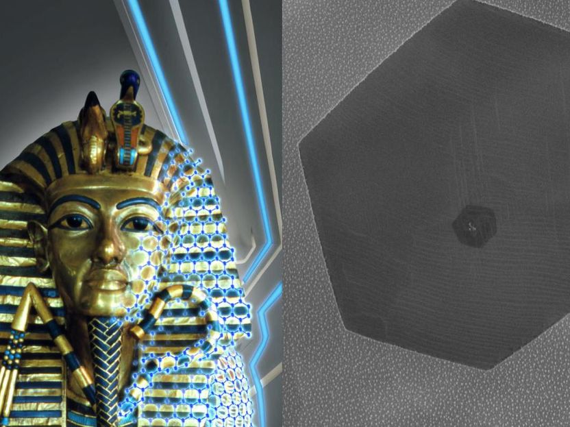
L: An artist rendering of graphene gilding on Tutankhamun's middle coffin (original photograph copyright: Griffith Institute, University of Oxford). R: Microscope image of a graphene crystal is shown on the palladium leaf. Although graphene is only a single atom thick, it can be observed in the scanning electron microscope. Here, a small crystal of graphene is shown to observe its edges. The team produces leaves where the graphene fully cover the metal surface.
Original photograph copyright: Griffith Institute, University of Oxford
In a new study, Sameh Tawfick, an assistant professor of Mechanical Science and Engineering at the University of Illinois at Urbana-Champaign, inspired by this ancient process, has added a single layer of carbon atoms, known as graphene, on top of metal leaves--doubling the protective quality of gilding against wear and tear.
The study, "Gilding with Graphene: Rapid Chemical Vapor Deposition Synthesis of Graphene on Thin Metal Leaves," is published in the journal Advanced Functional Materials. The researchers coated thin metal leaves of palladium with a single layer of graphene.
Metal leaves, or foils, offer many advantages as a scalable coating material, including their commercial availability in large rolls and their comparatively low price. By bonding a single layer of graphene to the leaves, Tawfick and his team demonstrated unexpected benefits, including enhanced mechanical resistance. Their work presents exciting opportunities for protective coating applications on large structures like buildings or ship hulls, metal surfaces of consumer electronics, and small precious artifacts or jewelry.
"Adding one more layer of graphene atoms onto the palladium made it twice as resistant to indents than the bare leaves alone," said Tawfick. "It's also very attractive from a cost perspective. The amount of graphene needed to cover the gilded structures of the Carbide & Carbon Building in Chicago, for example, would be the size of the head of a pin."
Additionally, the team developed a new technology to grow high-quality graphene directly on the surface of 150 nanometer-thin palladium leaves--in just 30 seconds. Using a process called chemical vapor deposition, in which the metal leaf is processed in a 1,100°C furnace, the bare palladium leaf acts as a catalyst, allowing the gases to react quickly.
"Chemical vapor deposition of graphene requires a very high temperature, which could melt the leaves or cause them to bead up by a process called solid state dewetting," said Kaihao Zhang, PhD candidate in MechSE and lead author of the study. "The process we developed deposits the graphene quickly enough to avoid high-temperature degradation, it's scalable, and it produces graphene of very high quality."
Original publication
Other news from the department science
These products might interest you
Dursan by SilcoTek
Innovative coating revolutionizes LC analysis
Stainless steel components with the performance of PEEK - inert, robust and cost-effective

OCA 200 by DataPhysics
Using contact angle meter to comprehensively characterise wetting behaviour, solids, and liquids
With its intuitive software and as a modular system, the OCA 200 answers to all customers’ needs
Tailor-made products for specific applications by IPC Process Center
Granulates and pellets - we develop and manufacture the perfect solution for you
Agglomeration of powders, pelletising of powders and fluids, coating with melts and polymers

Get the chemical industry in your inbox
By submitting this form you agree that LUMITOS AG will send you the newsletter(s) selected above by email. Your data will not be passed on to third parties. Your data will be stored and processed in accordance with our data protection regulations. LUMITOS may contact you by email for the purpose of advertising or market and opinion surveys. You can revoke your consent at any time without giving reasons to LUMITOS AG, Ernst-Augustin-Str. 2, 12489 Berlin, Germany or by e-mail at revoke@lumitos.com with effect for the future. In addition, each email contains a link to unsubscribe from the corresponding newsletter.
Most read news
More news from our other portals
Last viewed contents
Levorphanol
Celanese Secures Additional CO Supply at Nanjing Complex to Support Future Expansion
Rice University produces carbon-capture breakthrough - Porous material polymerizes carbon dioxide at natural gas wellheads
