Capturing light in a waveguide array
Advertisement
Cheaper and more efficient photonic devices, such as lasers, optical fibers, and other light sources may be possible with confined light that is unaffected by imperfections in the material that confines it, according to new research. A team of physicists from Penn State, the University of Pittsburgh, and the University of Illinois have demonstrated in a proof-of-concept experiment that they can contain light in such a way that makes it highly insensitive to defects that might be present in a material.

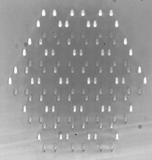
Microscope image of a cross-section of waveguide array in a topological crystalline insulator lattice geometry. New research shows that this configuration allows light to be confined in a way that is insensitive to imperfections in the material. This advance could lead to cheaper and more efficient photonic devices, such as lasers and optical fibers.
Rechtsman Laboratory, Penn State University
"Photonic technology involves the generation, transmission, and manipulation of light and it is used ubiquitously across industries," said Mikael Rechtsman, the Downsbrough Early Career Assistant Professor of Physics at Penn State and the leader of the research team. "It underlies the fiber optic network that forms the skeleton of the internet, solar cells used in the generation of sustainable energy, and high-power lasers used in manufacturing, among many other applications. Finding a way to confine and manipulate light so that it is insensitive to defects could have a huge impact on this technology."
To confine the light, the researchers used a complex lattice structure composed of "waveguides" precisely carved in glass. These waveguides act like wires, but for light instead of electricity. In this structure, light enters at one end of the waveguide and gets trapped and confined as it propagates forward through the wires. There, the trapped light becomes immune to imperfections in the positions of the waveguides, and thus significant imperfections in the structure can be tolerated.
"The light becomes insensitive because of the phenomenon of 'topological protection'," said Rechtsman. "This concept has been used extensively in the context of solid-state electronic physics. The waveguide structure is a photonic analogue of the so-called 'topological crystalline insulators,' and this form of topological protection can potentially be used across a range of photonic devices, including in nano-scale lasers, specialized nonlinear optical fibers, and for robustly and precisely coupling between photons and electrons for manipulating quantum information."
Confining light in this way could make many photonic devices at the same time cheaper to produce and more efficient. Beyond that, this is an example of the potentially cross-disciplinary--uniting photonics and solid-state electronics--use of topological protection and demonstrates the broad applicability of this phenomenon beyond its conception in electronic solid-state physics.
"In photonics, it is extremely important to be able to trap light and confine it to very small spaces," said Rechtsman. "It compresses the maximum amount of optical power into the smallest area or volume inside a material, making it interact more strongly with the material, and thus it is more efficient at whatever it is meant to do. A major difficulty with doing this has been that strong confinement brings with it extreme sensitivity to any imperfections in the material, which can often either inhibit efficiency or make the device very expensive to fabricate. Our results suggest that we can overcome this difficulty."


