Rare element to provide better material for high-speed electronics
Purdue researchers have discovered a new two-dimensional material, derived from the rare element tellurium, to make transistors that carry a current better throughout a computer chip.
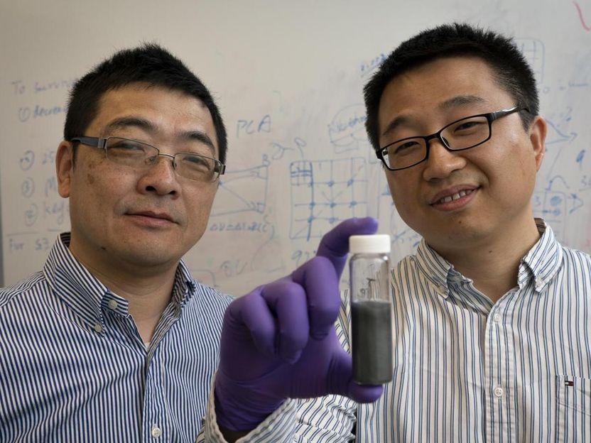
Purdue researchers Wenzhuo Wu and Peide Ye recently discovered tellurene, a two-dimensional material they manufactured in a solution, that has what it takes to make high-speed electronics faster.
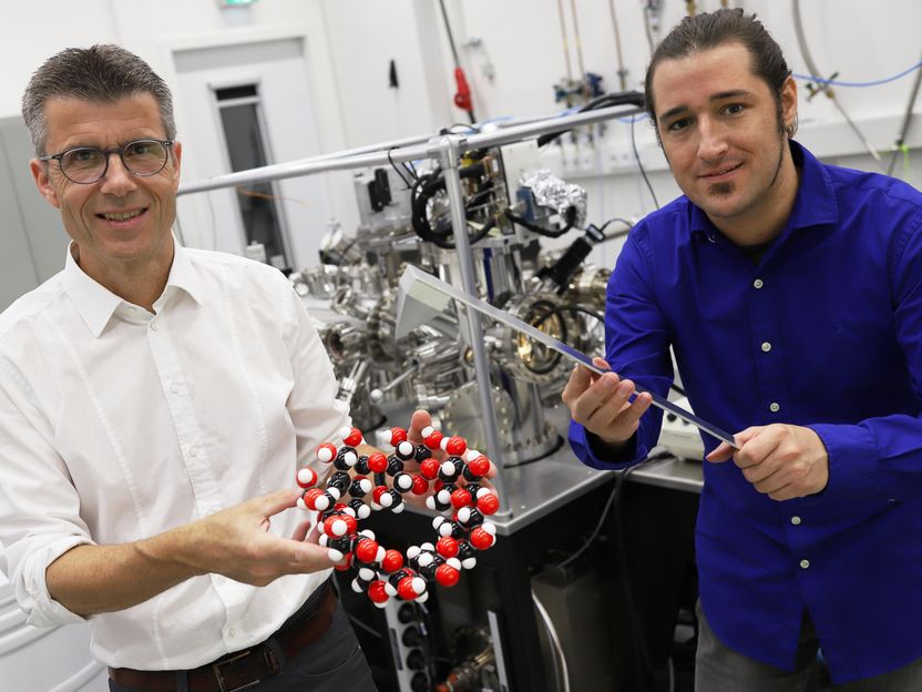
Purdue University image/Vincent Walter
The discovery adds to a list of extremely thin, two-dimensional materials that engineers have tried to use for improving the operation speed of a chip's transistors, which then allows information to be processed faster in electronic devices, such as phones and computers, and defense technologies like infrared sensors.
Other two-dimensional materials, such as graphene, black phosphorus and silicene, have lacked either stability at room temperature or the feasible production approaches required to nanomanufacture effective transistors for higher speed devices.
"All transistors need to send a large current, which translates to high-speed electronics," said Peide Ye, Purdue's Richard J. and Mary Jo Schwartz Professor of Electrical and Computer Engineering. "One-dimensional wires that currently make up transistors have very small cross sections. But a two-dimensional material, acting like a sheet, can send a current over a wider surface area."
Tellurene, a two-dimensional film researchers found in the element tellurium, achieves a stable, sheet-like transistor structure with faster-moving "carriers" - meaning electrons and the holes they leave in their place. Despite tellurium's rarity, the pros of tellurene would make transistors made from two-dimensional materials easier to produce on a larger scale.
"Even though tellurium is not abundant on the Earth's crust, we only need a little bit to be synthesized through a solution method. And within the same batch, we have a very high production yield of two-dimensional tellurene materials," said Wenzhuo Wu, assistant professor in Purdue's School of Industrial Engineering. "You simply scale up the container that holds the solution, so productivity is high."
Since electronics are typically in use at room temperature, naturally stable tellurene transistors at this temperature are more practical and cost-effective than other two-dimensional materials that have required a vacuum chamber or low operation temperature to achieve similar stability and performance.
The larger crystal flakes of tellurene also mean less barriers between flakes to electron movement - an issue with the more numerous, smaller flakes of other two-dimensional materials.
"High carrier mobility at room temperature means more practical applications," Ye said. Faster-moving electrons and holes then lead to higher currents across a chip.
The researchers anticipate that because tellurene can grow on its own without the help of any other substance, the material could possibly find use in other applications beyond computer chip transistors, such as flexible printed devices that convert mechanical vibrations or heat to electricity.
"Tellurene is a multifunctional material, and Purdue is the birthplace for this new material," Wu said. "In our opinion, this is much closer to the scalable production of two-dimensional materials with controlled properties for practical technologies."
Original publication
Yixiu Wang, Gang Qiu, Ruoxing Wang, Shouyuan Huang, Qingxiao Wang, Yuanyue Liu, Yuchen Du, William A. Goddard III, Moon J. Kim, Xianfan Xu, Peide D. Ye & Wenzhuo Wu; "Field-effect transistors made from solution-grown two-dimensional tellurene"; Nature Electronics; 2018
Most read news
Original publication
Yixiu Wang, Gang Qiu, Ruoxing Wang, Shouyuan Huang, Qingxiao Wang, Yuanyue Liu, Yuchen Du, William A. Goddard III, Moon J. Kim, Xianfan Xu, Peide D. Ye & Wenzhuo Wu; "Field-effect transistors made from solution-grown two-dimensional tellurene"; Nature Electronics; 2018
Organizations
Other news from the department science

Get the chemical industry in your inbox
By submitting this form you agree that LUMITOS AG will send you the newsletter(s) selected above by email. Your data will not be passed on to third parties. Your data will be stored and processed in accordance with our data protection regulations. LUMITOS may contact you by email for the purpose of advertising or market and opinion surveys. You can revoke your consent at any time without giving reasons to LUMITOS AG, Ernst-Augustin-Str. 2, 12489 Berlin, Germany or by e-mail at revoke@lumitos.com with effect for the future. In addition, each email contains a link to unsubscribe from the corresponding newsletter.
Most read news
More news from our other portals
Last viewed contents
Amino_acid
Quartz_diorite
Brunner_Mond
ADAMTS13
Self-amplifying selectivity
Steady_flow
PEG_400
Mitochondrial_Eve
Discover 2.0 | Microwave synthesizers | CEM
