A New Way to Atomically Thin Materials
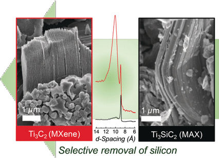
Silicon secedes: titanium carbide flakes obtained by selective etching of titanium silicon carbide
Metallic conductivity and hydrophilicity of MXenes have established them as electrodes in rechargeable batteries and supercapacitors, as well as other applications, including photothermal cancer therapy, electromagnetic shielding, water purification and gas sensing. In the journal Angewandte Chemie, researchers have now introduced a new production method. Instead of using conventional, yet more expensive, titanium aluminum carbide, they selectively etch silicon out of titanium silicon carbide, a cheaper and more common precursor, to synthesize titanium carbide.

© Wiley-VCH
Two-dimensional materials, consisting of extremely thin layers that are a few atoms thick, have unique properties that are completely different than the normal three-dimensional versions. A prominent example of this is graphene, which is made of single layers of carbon atoms. In 2011, a new class of two-dimensional materials was synthesized at Drexel University in Philadelphia (Pennsylvania, USA). Known as MXenes, the materials are made of transition metal carbides and nitrides, where the M stands for a transition metal, such as titanium, vanadium, or molybdenum, X can be carbon and/or nitrogen, and many compositions are available (about 30 have already been experimentally demonstrated and dozens more are expected). One such MXene is titanium carbide, Ti3C2.
Obtaining the desired MXene usually involves a roundabout process: Layered carbides and nitrides, known as MAX phases, are selectively etched with hydrofluoric acid to remove the layers of the “A” element, which is a group 13 or 14 element such as aluminum, silicon, or germanium. In this way, titanium carbide can be obtained by etching the aluminum out of titanium aluminum carbide (Ti3AlC2). However, this starting material is expensive, and the production is complex. In contrast, the silicon analog, titanium silicon carbide (Ti3SiC2), is commercially available and less expensive. Ti3SiC2 was the first MAX phase Drexel researchers tried to selectively etch in 2011, but synthesis failed using hydrofluoric acid alone because the silicon atoms are strongly bound to the adjacent transition metal atoms.
A team led by Yury Gogotsi at Drexel University has now developed a successful variation of this process. By adding an oxidizing agent, the researchers could weaken the silicon bonds and oxidize silicon. Using mixtures of hydrofluoric acid and an oxidizing agent like nitric acid, hydrogen peroxide, or potassium permanganate, the team produced titanium carbide MXene by selectively removing silicon out of Ti3SiC2.
The etching process leaves behind stacks of titanium carbide, which can be delaminated to make flakes, which are approximately 1 nanometer in thickness. The researchers used this method to make flexible, electrically conducting titanium carbide films on a relatively large scale.
This new method could make the production of MXenes easier, and open pathways to the production of new MXenes and related two-dimensional materials from silicon-containing precursors, expanding the family of 2D nanosheets available to scientists and engineers.
Original publication
Other news from the department science

Get the chemical industry in your inbox
By submitting this form you agree that LUMITOS AG will send you the newsletter(s) selected above by email. Your data will not be passed on to third parties. Your data will be stored and processed in accordance with our data protection regulations. LUMITOS may contact you by email for the purpose of advertising or market and opinion surveys. You can revoke your consent at any time without giving reasons to LUMITOS AG, Ernst-Augustin-Str. 2, 12489 Berlin, Germany or by e-mail at revoke@lumitos.com with effect for the future. In addition, each email contains a link to unsubscribe from the corresponding newsletter.
Most read news
More news from our other portals
Last viewed contents
FUTBOLIN

New method measures 3D polymer processing precisely
Clean_Energy_Partnership
Abeles_matrix_formalism
Apokjeden
Gaussian_broadening
Tiny sensors tucked into cell phones could map airborne toxins in real time
General_Motors_Sequel


