Germanium outperforms silicon in energy efficient transistors with n- und p- conduction
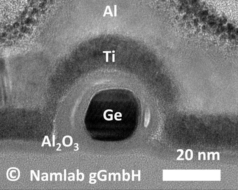
A team of scientists from the Nanoelectronic Materials Laboratory (NaMLab gGmbH) and the Cluster of Excellence Center for Advancing electronics Dresden (cfaed) at the Dresden University of Technology have demonstrated the world-wide first transistor based on germanium that can be programmed between electron- (n) and hole- (p) conduction. transistors based on germanium can be operated at low supply voltages and reduced power consumption, due to the low band gap compared to silicon. Additionally, the realized germanium based transistors can be reconfigured between electron and hole conduction based on the voltage applied to one of the gate electrodes. This enables to realize circuits with lower transistor count compared to state-of-the-art CMOS technologies.

Energy-efficient germanium nanowire transistor with programmable p- and n- conduction. Transmission electron microscope image of cross section.
NaMLab gGmbH
Today´s digital electronics are dominated by integrated circuits built by transistors. For more than four decades transistors have been miniaturized to enhance computational power and speed. Recent developments aim to maintain this trend by employing materials having higher mobility than silicon in the transistor channel, like germanium and indium-arsenide. One of the limitations in using those materials is the higher static power loss in the transistor´s off-state, also originating from their small band gaps. The scientist team around Jens Trommer and Dr. Walter Weber from NaMLab in cooperation with cfaed succeeded in solving this issue by conceiving the germanium-nanowire transistor with independent gating regions. Dr. Weber who leads cfaed’s Nanowire Research Group points out: “For the first time the results demonstrate the combination of low operation voltages with reduced off-state leakage. The results are a key enabler for novel energy efficient circuits.”
The work has been supported by the German Research Foundation (DFG) in the project ReproNano and has been performed in close cooperation with the DFG Cluster of Excellence Center for Advancing Electronics Dresden (cfaed). NaMLab will strive for further implementation in future products as well as further advancement in R&D with its industrial partners.
Original publication
Other news from the department science

Get the chemical industry in your inbox
By submitting this form you agree that LUMITOS AG will send you the newsletter(s) selected above by email. Your data will not be passed on to third parties. Your data will be stored and processed in accordance with our data protection regulations. LUMITOS may contact you by email for the purpose of advertising or market and opinion surveys. You can revoke your consent at any time without giving reasons to LUMITOS AG, Ernst-Augustin-Str. 2, 12489 Berlin, Germany or by e-mail at revoke@lumitos.com with effect for the future. In addition, each email contains a link to unsubscribe from the corresponding newsletter.


