New material could lead to erasable and rewritable optical chips
A military drone flying on a reconnaissance mission is captured behind enemy lines, setting into motion a team of engineers who need to remotely delete sensitive information carried on the drone's chips. Because the chips are optical and not electronic, the engineers can now simply flash a beam of UV light onto the chip to instantly erase all content. Disaster averted.

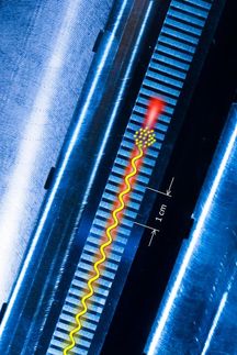
This image is a video still that shows the researchers rewriting a waveguide, a component that guides light, using a laser on nanomaterial. (The waveguide is the horizontal line on the box.)
Cockrell School of Engineering
This James Bond-esque chip is closer to reality because of a new development in a nanomaterial developed by Yuebing Zheng, a professor of mechanical engineering and materials science and engineering in the Cockrell School of Engineering.
"The molecules in this material are very sensitive to light, so we can use a UV light or specific light wavelengths to erase or create optical components," Zheng said. "Potentially, we could incorporate this LED into the chip and erase its contents wirelessly. We could even time it to disappear after a certain period of time."
To test their innovation, the researchers used a green laser to develop a waveguide -- a structure or tunnel that guides light waves from one point to another -- on their nanomaterial. They then erased the waveguide with a UV light, and re-wrote it on the same material using the green laser. The researchers believe they are the first to rewrite a waveguide, which is a crucial photonic component and a building block for integrated circuits, using an all-optical technique.
Their main advancement is a specially designed hybrid nanomaterial that is akin to a child's Etch-A-Sketch toy -- only the material relies on light and tiny molecules to draw, delete and re-write optical components. Engineers and scientists are interested in rewritable components that use light rather than electricity to carry data because they hold potential for making devices faster, smaller and more energy-efficient than components made from silicon.
The concept of rewritable optics, which underpins optical storage devices such as CDs and DVDs, has been pursued intensely. The drawback to CDs, DVDs and other state-of-the-art rewritable optical components is that they require bulky, stand-alone light sources, optical media and light detectors.
In contrast, the UT Austin innovation allows for writing, erasing and rewriting to all happen on the two-dimensional (2-D) nanomaterial, which paves the way for nano-scale optical chips and circuits.
"To develop rewritable integrated nanophotonic circuits, one has to be able to confine light within a 2-D plane, where the light can travel in the plane over a long distance and be arbitrarily controlled in terms of its propagation direction, amplitude, frequency and phase," Zheng said. "Our material, which is a hybrid, makes it possible to develop rewritable integrated nanophotonic circuits."
The researchers' material starts with a plasmonic surface, which is made up of aluminum nanoparticles, on top of which sits a 280-nanometer polymer layer embedded with molecules that can respond to light. Due to quantum mechanics interactions with the light, the molecules can either become transparent, allowing the light waves to propagate, or they can absorb the light.
Another advantage of the material is that it can operate two light-transporting modes simultaneously -- called the hybrid mode. The material's dielectric waveguide mode can guide light propagation over a long distance, while the plasmonic mode is able to dramatically amplify the light signals within a smaller space.
"The hybrid mode takes the advantages of both dielectric waveguide mode and plasmonic resonance mode, and combines them together while circumventing the limits of each," Zheng said. "We realized an all-optical control through a technique, called photoswitchable Rabi splitting, which, for the first time, can be achieved in the hybrid plasmon-waveguide mode."
The integration between these two modes significantly improves the performances of the optical cavity in this hybrid nanomaterial, which features high quality factor and low optical loss and thus maximizes the coupling between the molecules and the hybrid mode.
There are challenges that must be addressed before an optical chip or nanophotonic circuit can be designed using this material, Zheng said, including optimizing the molecules to improve the stability of the re-writable waveguides and their performance for optical communications.


